|
Detector
High resistivity, fully depleted CCDs Fig. 1: a) DAMIC-M CCD module in its low-background package.
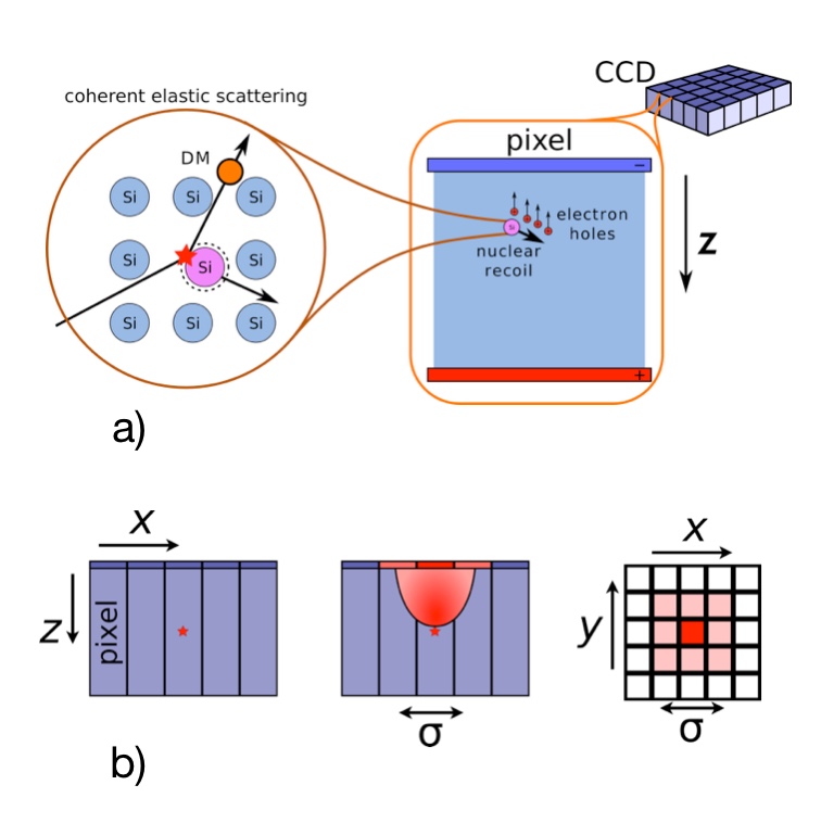
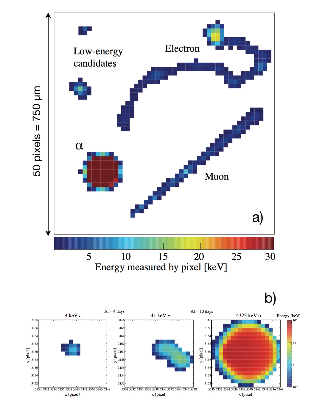
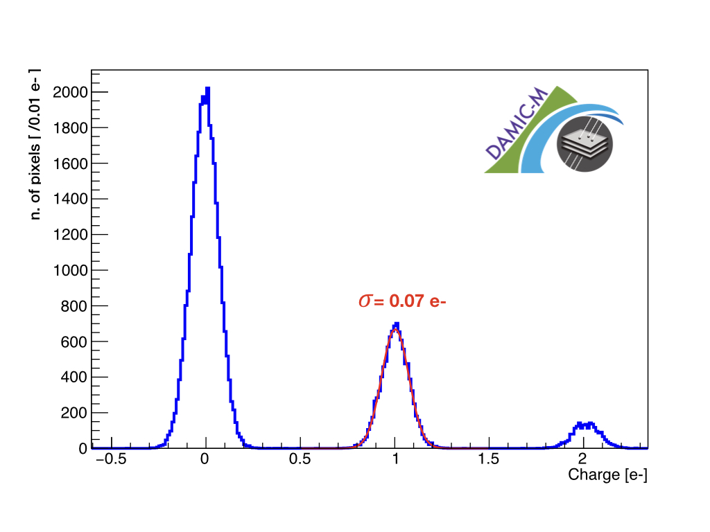
Four CCDs are glued on a silicon pitch adapter with traces bringing voltages to the CCDs from the flex cable; b) cross section of a high-resistivity fully depleted CCD. The DAMIC-M CCDs were developed by Lawrence Berkeley National Laboratory (LBNL). They have a record thickness of 675 μm and active area of 9.2 cm x 2.3 cm, for a mass of 3.2 g each. A DAMIC-M module consists of four of these CCDs, glued on a silicon substrate (Fig. 1.a). The detectors are fabricated from n-type, high-resistivity (>10,000 Ω cm) silicon wafers, and are fully depleted (i.e., active over their full volume) by applying a potential (≥ 40 V) to a thin back-side contact (Fig. 1.b). The 15 μm x 15 μm pixels have a conventional 3-phase polysilicon gate structure to hold and transfer the charge, arranged in an array of 6144 x 1536 pixels pixels. In the serial readout process, the charge is transferred vertically from pixel to pixel along each column by appropriate clocking of the 3-phase gates until it reaches the last row (“serial register”); higher frequency clocks move the charge horizontally until the end of the serial register where the on-chip charge-to-voltage amplifier is located. The corresponding voltage signal is then processed to determine the pixel charge. A readout noise of ≈ 3.2 electrons for a single pixel charge measurement has been achieved in the Low Background Chamber at the LSM. The skipper readout (see below) reduces this noise to a sub-electron level CCDs as Dark Matter detectors Fig. 2: a) DM detection in a CCD; b) 3D position reconstruction. The principle of DM detection with a CCD is illustrated in Fig. 2.a. The charge produced in the DM particle interaction, through absorption or a nuclear/electronic recoil, drifts towards the pixel gates, where it is held in place until the readout. The ionized charge diffuses transversely as it is drifted toward the pixel gates, with a spatial variance that is proportional to the transit time (Fig. 2.b). Hence, there is a positive correlation between the lateral diffusion of the collected charge on the pixel array and the depth of the interaction, which can be used for three-dimensional position reconstruction. Background identification and rejection Fig.3. a) signatures of different ionizing particles in a CCD: a straight track (cosmic ray muon), large blob (alpha particle), “worm” (straggling electron) and small round clusters (low-energy X-ray, nuclear recoil, DM candidate); b) the decay chain of a single 210Pb nucleus on the CCD surface: a sequence of two beta and one alpha particle separated in time by several days and detected in the same location Surface backgrounds, which arise from low-energy photons and electrons emitted by radioactive decay on surfaces or radiated by the surrounding materials, are efficiently rejected by 3D reconstruction. Also, the characteristics of the clusters readily identify the nature of the ionizing particles (Fig. 3.a) providing important information of the origin of the background. A truly unique capability of DAMIC-M is that background can be identified and rejected as spatially correlated events occurring at different times. An example is shown in Fig. 3.b, with three clusters (two electrons and one alpha) detected in the same location but separated in time by several days. The probability for this to occur by chance is negligible. Rather, the observation is consistent with a 210Pb nucleus undergoing the decay sequence 210Pb (T 1/2= 22.3 y, β) → 210Bi (T 1/2=5.0 days, β) → 210Po (T 1/2= 138 days, α). A product of the radon decay chain, 210Pb is a major source of surface background in DM experiments caused by material exposure to air. This background rejection capability is also particularly relevant for 32Si, a naturally occurring isotope in silicon that is not removed by chemical purification, which is expected to be the dominant background contribution in the current generation of silicon detectors. DAMIC-M identifies and rejects by spatial correlation the decay sequence 32Si (T 1/2= 150 y, β) → 32P (T 1/2= 14 days, β). Skipper CCDs with single-electron resolution Fig.4. Pixel charge distribution for a prototype DAMIC-M CCD with skipper readout: pixels with zero, one, two electrons are counted with high resolution (0.07 e- from the width of the Gaussian peaks). The crucial innovation in DAMIC-M is the integration on these large devices of a novel on-chip readout scheme, where sub-electron noise is achieved by a non-destructive, multiple measurement of the pixel charge. In the so-called “skipper” readout, the charge of a pixel is measured N times, and by taking the average of these measurements the white noise is reduced by √N. Most importantly, the effect of low-frequency 1/f noise is drastically reduced, since the integration time of each measurement is much shorter than in the conventional readout. The pixel charge distribution from a DAMIC-M skipper CCD is shown in Fig. 4, with well-separated peaks corresponding to zero, one, two, etc. electrons. With a noise of only ≈ 0.1 e-, DAMIC-M detects with high-resolution a single electron. Thus, it is sensitive to extremely small energy transfers from a DM-electron interaction, since 1.1 eV (band gap energy) is the threshold to produce an electron-hole pair in silicon (with 3.7 eV required on average). Even with single-charge resolution, a signal may remain hidden in the fluctuations of the detector’s dark current. DAMIC CCDs have the lowest dark current ever measured in a silicon detector, ≤ 2x10 -22 A/cm 2 at an operating temperature of 140 K. DAMIC-M at the Laboratoire Souterrain de Modane Fig. 5: the DAMIC-M experiment at the LSM; a) the CCD array, with 52 CCD modules; b) cross section of the DAMIC-M apparatus, with major components DAMIC-M is being installed at the Laboratoire Souterrain de Modane in France, protected from cosmic rays by the rock overburden of the Alps. In addition, the horizontal access through the Frejus tunnel simplifies the logistics to perform detector packaging, test and assembly underground. Supply of radon-free air to minimize surface backgrounds is part of the laboratory infrastructure. The DAMIC-M design is shown in Fig. 5. A cryostat vessel houses the CCDs, closely packed in CCD array surrounded by a infrared (IR) shield. Cooling is provided by a copper cold finger connected to a cryocooler located outside the shielding. The upper part of the vacuum cryostat, the IR shield, and the CCD array support are made of electroformed copper to minimize radiogenic backgrounds. The cryostat is enclosed in a 20-cm-thick lead shielding to stop high-energy radiogenic photons from the external environment. Standard lead contains quantities of 210Pb (T 1/2 = 22 years, β) whose decay chain products may generate penetrating bremsstrahlung photons escaping the shield. For this reason, the innermost 5 cm of the shield are made of ancient lead available at the LSM, recovered from a Roman ship sunk in Brittany in 400 A.C. The entire lead shield is enclosed by 40-cm-thick polyethylene to efficiently stop external neutrons.
|